
Stage 01
Stage 01 of 07 · ← / → to navigate
IP / Architecture
Define reusable IP and subsystem architecture.
Engineering outcome
Architecture aligned to the product requirement.
IP architecture
Subsystem definition
Semiconductor engineering from IP to Silicon across RTL Design, Design Verification, Physical Design, DFT, Protocol Verification and SoC & IP Engineering.
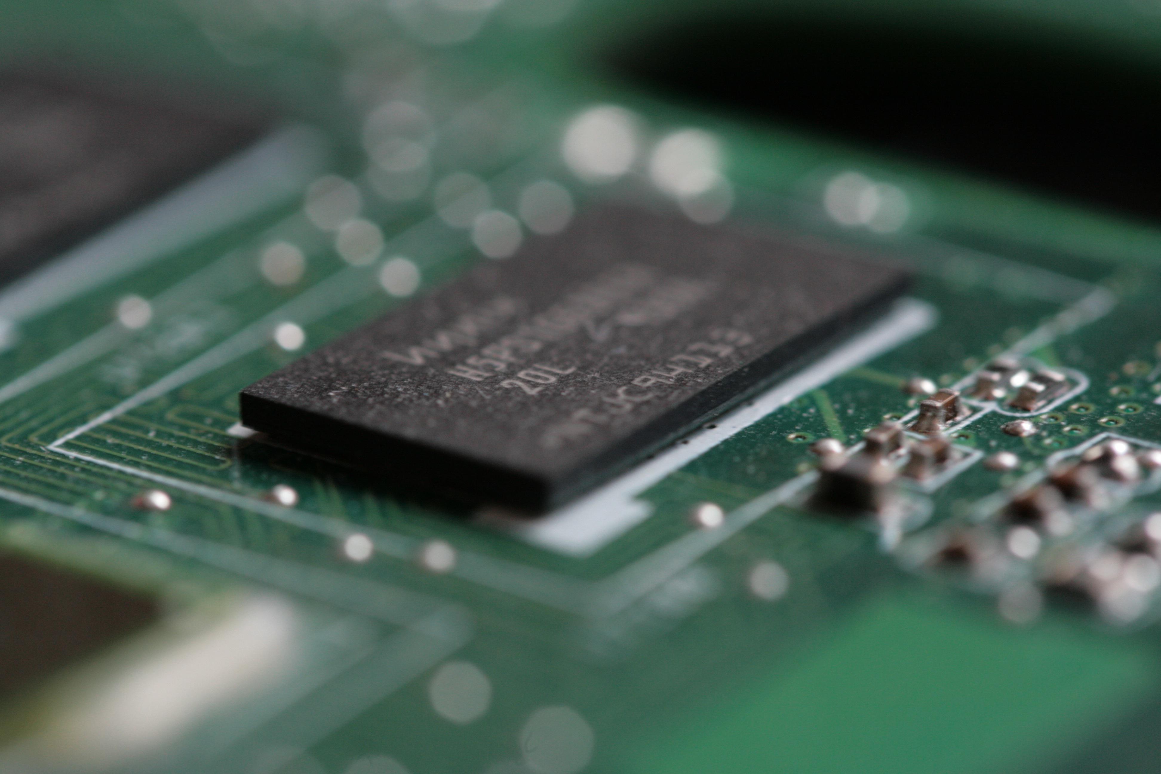
Engineering expertise across the semiconductor development lifecycle.
Explore each stage to see where AionSi engineering contributes.
Define reusable IP and subsystem architecture.
Architecture aligned to the product requirement.
Need engineering capacity at any stage of the silicon lifecycle?
Talk to Our Engineering TeamFrom RTL design through verification, physical implementation, DFT, protocol verification and SoC integration—AionSi engineering capabilities are built around complex silicon programs.
RTL engineering across block, subsystem and SoC development.
Verification expertise across block, subsystem and SoC levels.
Physical implementation, timing closure and physical verification across complex silicon programs from netlist through sign-off.
Design-for-test engineering integrated into the silicon lifecycle.
Protocol-focused verification for complex semiconductor interfaces.
Engineering across processor, interconnect, memory, security and high-speed protocol IP with SoC integration.
Bring a verification, implementation or engineering-capacity challenge. We will connect it to the right AionSi capability.
A focused set of technology domains backed by supplied AionSi technical capability evidence.
Each technology card now maps to an evidence-backed reference. Unsupported or lower-confidence technology claims are intentionally excluded from this section.
Production-grade Data Link Layer engineering with link training, flow control, error recovery, power management and SoC integration.
Integrated USB controller engineering spanning PHY, link and protocol layers, power delivery, error recovery and host/device integration.
Memory-controller engineering covering command scheduling, PHY abstraction, refresh management, ECC/RAS, timing and SoC integration.
High-bandwidth memory controller engineering for AI, GPU and HPC systems with QoS-aware scheduling and thermal-aware integration.
Coherent and non-coherent interconnect engineering for heterogeneous SoCs with QoS, configurable topology, monitoring and scalable agent counts.
Processor-core engineering spanning embedded, edge-AI, performance and multi-core cluster tiers with formal and dynamic verification.
Engineering productivity accelerated with human validation, security-conscious workflows and controlled deployment models.
Dedicated engineering teams, extended engineering and project delivery models designed around semiconductor programs.
Trusted by leading organizations across semiconductor, EDA, automotive, networking and technology markets.







AionSi is building an engineering organization for complex silicon programs. Explore opportunities for early-career and experienced semiconductor engineers.
Build semiconductor fundamentals, learn engineering methodologies and grow with experienced teams.
Work on challenging semiconductor programs across verification, physical design, RTL, DFT and protocol engineering.